
Industrial solution
Photovoltaics
From wafer intake through to module EL inspection.

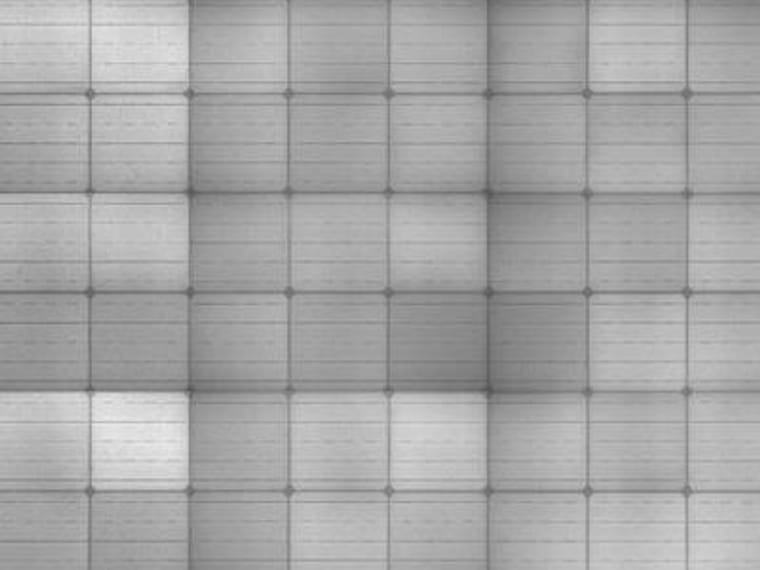
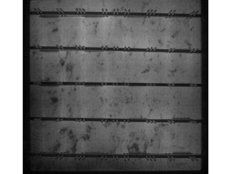
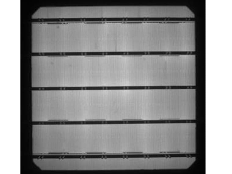
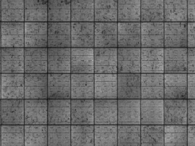
Defect detection in cells and modules bears directly on yield. Conventional algorithms handle a single defect type well but generalise poorly to compound defects that vary in shape and scale. DSTEK detects them automatically in electroluminescence imagery, and supplies the wafer loading and unloading automation alongside.
Scope
What we inspect
-
Wafer intake
Size, saw marks, bow, breakage, micro-cracks and contamination; breakage, overlap and angle during basket insertion
-
Post-PECVD
Coating colour variation and surface defects — white spots, contamination, intra- and inter-cell colour difference, edge bow, etch marks
-
Screen printing
Grid breaks, print offset, line width, back-field delamination, paste leakage
-
PL / EL
Back-film contamination and suction marks, front-film scratches and white spots, post-print micro-cracks
-
Module EL
Linear and cross micro-cracks, black corners, black spots
-
Wafer handling
Loading and unloading automation; breakage, overlap and angle on basket insertion
Applications
Representative inspection tasks
A selection of what we have actually run on the line — not the full list. New inspection targets are approached the same way.
-
Mono/poly wafer inspection
Size, saw marks, bow, breakage, micro-cracks, contamination
-
Vertical basket inspection
Fragments, wrong wafers, overlapped or thick wafers, insertion imbalance (height difference over 20mm)
-
PECVD coating inspection
White spots, contamination, intra-cell and overall colour difference, edge bow, etch marks
-
SE electrode cell inspection
Two-dimensional reference deviation of ±15μm
-
Screen print inspection
Grid breaks, print offset, line width, back-field delamination, back-electrode offset, paste leakage
-
Cell colour sorting
Crystalline silicon colour depth and distribution, sorted into 8–24 trays
-
Junction box laser welding
Weld head guidance, busbar flatness inspection, post-weld quality inspection
-
Module string welding EL
Linear and cross micro-cracks, black corners and spots
-
Automatic wafer loading/unloading
Solar wafer loading and unloading line automation
Inspection imagery
What the system sees
-
-
-
-


Our edge
What we bring to this industry
- 01 Deep-learning models built specifically for EL and PL imagery
- 02 Precision measurement to a ±15μm reference
- 03 Inspection and wafer handling automation supplied as one line
Other industries
Explore the other industries we serve
What runs this inspection