
Industrial solution
Semiconductor & Substrates
Wafer, package and bonding through to PCBA, FPC and FC-BGA.

Semiconductor packaging is fine-pitch work with complex defect modes, so inspection has to be both precise and fast. Substrates keep shrinking and densifying, and conventional AOI can no longer hold down over- and under-detection. DSTEK combines 2D/3D imaging, multi-colour multi-angle strobe capture and a PCB-specific industrial AI model to cover everything from the wafer to the assembled board.
- Over 50Compatible product types
- 1μmMeasurement precision
- 20+FPC defect types
Scope
What we inspect
-
Wafer
Bump height, diameter, pitch and coplanarity; surface scratches, contamination and foreign matter
-
BGA / QFP / QFN
Solder ball height, pitch and coplanarity; missing balls, cracks, bridging; lead skew and coplanarity
-
Wire bonding
Wire and pad offset, loop faults, sagging, lifting; bridging, missing and double bonds
-
PCBA
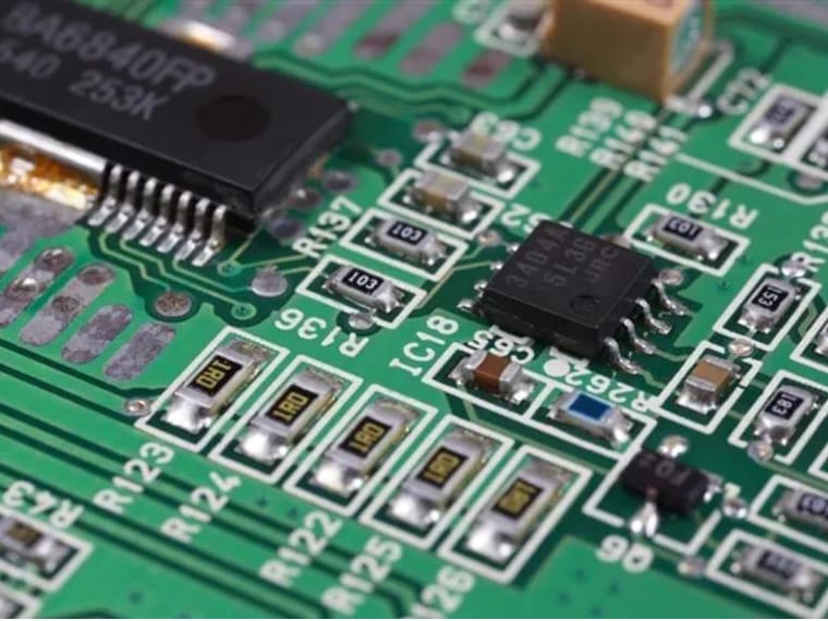
Insufficient and excess solder, bridging, cold joints and voids quantified at pixel level; wrong, missing and reversed parts
-
FPC / FPCA
Creases, folds, gold-finger curvature, plating bridges, exposed copper, tears — 20+ defect types
-
FC-BGA
Contamination, scratches, pits, bubbles, white spots and hole defects; ring width and bonding pad dimensions
Applications
Representative inspection tasks
A selection of what we have actually run on the line — not the full list. New inspection targets are approached the same way.
-
Wafer appearance inspection
Dicing anomalies, pad protrusion, defects and scratches, edge damage, delamination, chip residue, emitting-area defects
-
Chip appearance and dimensions
Contamination, spots, damage, corner defects, foreign matter, missing parts, misalignment, counting
-
SMT solder joint inspection
Insufficient solder, excess solder, bridging and shorts, cold joints, voids
-
Lead frame inspection
QFN plated silver and copper surfaces — staining, yellowing, discolouration, silver leakage, under- and over-etching
-
Capacitor inspection
Polarity reversal, mixed capacitance, unclear sleeve marking, aluminium case deformation
-
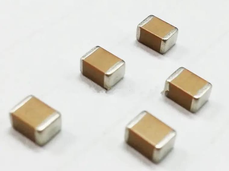
MLCC appearance inspection
Six-sided cracks, chipping, contamination and electrode defects
-
Inductor six-sided AOI
Dents, cracks, warping, gaps, contamination, grit, burrs, bubbles, colour non-uniformity
-
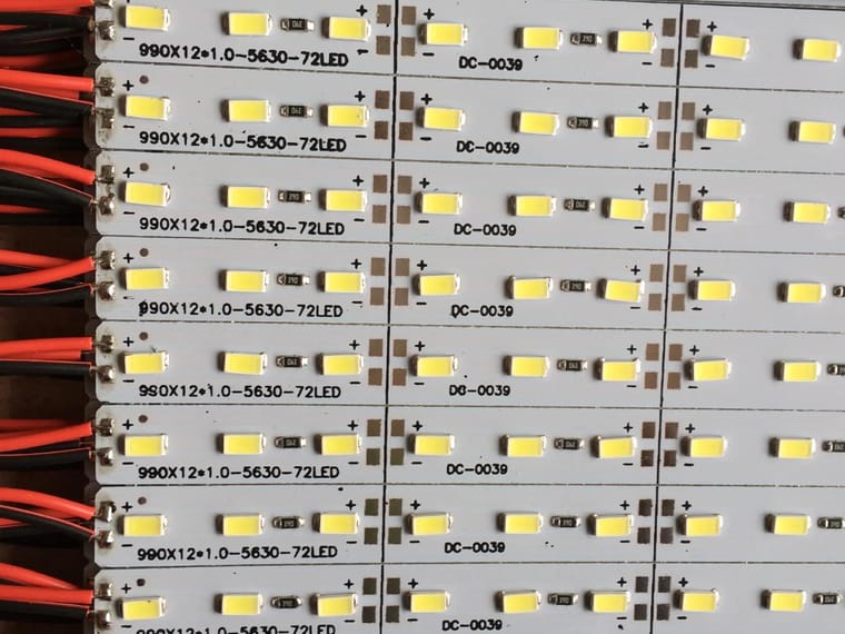
LED lamp bead inspection
Excess and insufficient adhesive, bubbles, cracks and scratches on the bond line, pin deformation and absence
-
Precision resistor inspection
Base contamination, silver leakage, insufficient silver on the top face
-
Connector appearance inspection
Male and female connector solder defects and joint offset
Global semiconductor and component manufacturer
Inspection imagery
What the system sees
-
-

-
-


Our edge
What we bring to this industry
- 01 A PCB-specific industrial AI model compatible with over 50 product types
- 02 Multi-colour, multi-angle strobe imaging resolves fine solder defects
- 03 Pixel-level segmentation quantifies defect area to 1μm precision
Other industries
Explore the other industries we serve
What runs this inspection